NAND scaling is at the heart of data storage innovation. As AI workloads, hyperscale infrastructure, and connected devices continue to proliferate, so do the demands on compute, memory, and storage. Continued progress will depend heavily on increasing NAND density, performance, and efficiency—all without expanding the physical footprint or escalating costs.
With the advent of 3D NAND more than a decade ago, the industry has found a way to continually push the boundaries of Flash technology further. But each method of scaling NAND has tradeoffs. Thus, to continue the march of progress, Sandisk explores NAND scaling across four critical vectors: lateral, logical, vertical, and architectural.
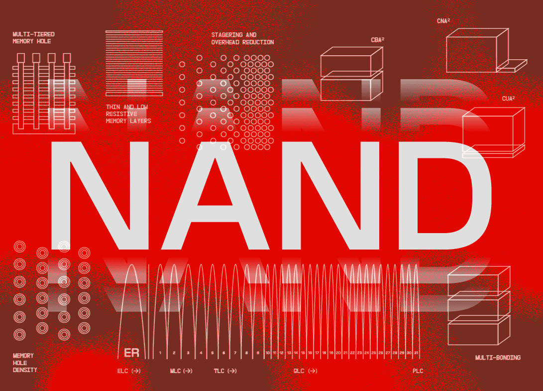
What Is NAND Scaling?
Scaling in NAND technology refers to the process of increasing storage capacity while maintaining or even reducing physical size, thereby optimizing performance without substantially increasing power consumption or cost.
A significant contributing factor to the successful innovation of the technology was the introduction of 3D NAND. As devices continually became smaller while demands for storage capacity and performance increased, 2D NAND reached a limit where components could be shrunk only so small.
“The physics of building devices smaller and smaller became very, very difficult”, said Alper Ilkbahar, Sandisk EVP and CTO, at Sandisk’s Investor Day in February this year. “We got around that problem by inventing 3D NAND and stacking devices on top of each other vertically. [As a result], 3D NAND is one of the most scalable semiconductor technologies in the world.”
But merely scaling vertically also comes with certain limitations. Thus began a technological journey to explore alternative methods for scaling, embracing innovative techniques to overcome physical limitations, and enabling exponential growth in NAND capabilities.
Lateral Scaling
Lateral scaling aims to utilize the horizontal space of the memory chip as efficiently as possible. This is achieved through methods that include reducing the pitch (spacing) between memory cells by shrinking the horizontal spacing and optimizing cell placement, as well as optimizing peripheral circuit areas by implementing architectures like CMOS-under-array.
“What we mean by lateral scaling is how many bits we can pack in every square millimeter of every memory layer”, Ilkbahar said. As the most linear of all the vectors, the more bits per millimeter that are added, the bit growth and cost reduction per bit grow at a near one-to-one ratio.
Ilkbahar also noted that lateral scaling is one of the most technologically challenging methods because, as cells are packed closer together, interference and error rates can increase, necessitating more advanced and precise manufacturing methods.
Logical Scaling
Logical scaling refers to the number of bits of data that can be stored in a single NAND cell. Instead of storing just one bit per cell, modern NAND technologies can store multiple bits, like QLC, which stores four bits in each cell by using more precise levels of charge.
This increases storage capacity and lowers the cost per gigabyte, but it also introduces trade-offs in areas like speed, reliability, and endurance. Many of these challenges can be addressed through system-level improvements and by designing the technology for specific, targeted use cases.
“We do this by carefully optimizing process and device parameters, as well as deploying signal processing and error correction algorithms at a system level”, Ilkbahar said. “This very organic and intimate relationship between system and device design really makes this possible.”
Vertical Scaling
The shift to 3D NAND represents one of the most revolutionary steps in Flash development. With 2D NAND, scaling was primarily achieved through lateral methods, where components were shrunk to smaller and smaller sizes to fit more of them side by side. Eventually, though, it became nearly impossible to keep shrinking components physically. With 3D NAND, scaling is achieved vertically by stacking layers of semiconductor material on top of one another, much like a skyscraper in a city, as opposed to a suburban housing division with single homes on each lot of land. Memory cells are designed to stack on top of one another, allowing for staggering density increases without significantly expanding the physical footprint.
Adding more layers does require substantial investment in additional specialized manufacturing equipment to etch precise, high-aspect-ratio holes in silicon wafers. As such, while manufacturing complexity increases with the addition of more layers, the cost per gigabyte typically continues to improve through the combination of scaling methods, although challenges like wafer warping present technical hurdles.
Architectural Scaling
Lastly, architectural scaling focuses on the layout of the circuits that support the memory arrays. While there are multiple, different ways to architect these circuits that control the memory arrays, Sandisk and Kioxia jointly introduced a novel approach with the introduction of BiCS8, called CBA (CMOS directly Bonded to Array).
CMOS circuitry, the logic that controls the memory cells, was previously produced on the same wafer as the NAND array. However, NAND and CMOS typically prefer different thermal and processing parameters during their construction. When CMOS is built under the array (CUA), the subsequent high-temperature NAND processing steps impose a "thermal budget" limitation on the CMOS, preventing its full optimization. With CBA, the memory arrays and circuits are built on separate wafers, allowing them to be optimized individually. The two wafers are then bonded together.
“When you build these wafers separately, you can optimize them separately and get the best of both worlds — higher performing cells and higher performing circuits,” Ilkbahar said. “This is how we achieve exceptional performance."
As a proving point, Ilkbahar, during his presentation at the February 2025 Investor Day conference, held up the newest QLC memory die, which utilizes CBA technology to achieve a 2TB capacity1, the largest in production at the time.
Scaling the Future
While some vectors of scaling have advantages over others, Ilkbahar emphasized the importance of exploring them, particularly those he asserts are most productive for customers.
“Our focus is on the most productive vectors—lateral, logical, and architectural—in all of which we help lead in the industry”, he said. “When it comes to vertical scaling and adding layers, of course, we will continue adding layers. But our priority is going to be delivering cost and performance leadership [by] pursuing the other vectors.”
This approach to scaling lays out Sandisk’s roadmap for advancing bit density. Rather than defaulting to stacking additional layers to achieve density and cost reduction, engineering teams at Sandisk are exploring what customers need from NAND and designing ways to scale via the methods that make the most economic sense, which he says will maintain the company’s leadership in both CAPEX efficiency and cost leadership.
To learn more about CBA and the 10th generation of 3D Flash, read the joint press release from Kioxia and Sandisk.
You can also watch the entire Investor Day presentation here.