|

The Hidden Math Behind Reliable Flash Storage
In the race to store more data in smaller spaces, the industry has long focused on physical scaling—shrinking silicon, stacking layers, and packing more bits into memory cells. But as flash memory becomes denser, it also becomes more fragile. Then, as physical limits tighten, innovation has also shifted to something less visible: math.
Tricky bits
In Kfar Saba, a tree-lined Israeli suburban high-tech hub, Dr. Eran Sharon leads a team of technologists from around the globe. A Distinguished Engineer in Sandisk's R&D Engineering, Dr. Sharon has been pioneering advanced algorithms for over three decades.
"People are probably unaware of the complex algorithms and advanced math involved in every presumably simple operation of storing or reading data from their memory device," Dr. Sharon said.
While our always-connected world assumes the flawless flow of digital information, behind the scenes, things look very different. Because every time data moves—whether saved, read, or transmitted—it faces a spate of corrupting influences that jumble the original state of the 1s and 0s that make up our data.
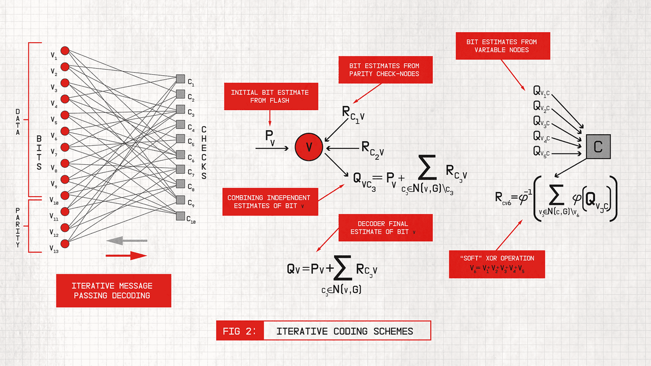
Information theory, which emerged in the 1940s, laid the groundwork for fixing these bit errors with math. Just like a spell checker uses context and rules to correct typos, error correction codes rely on mathematical schemes to detect which bits got flipped and how to fix them.
"Error Correction Codes (ECC) work by adding redundant bits that describe attributes of the original data," Dr. Sharon said.
He explained that the most common approach is to add parity bits. Parity bits indicate whether the number of 1s within predefined subsets of the bits is odd or even. Adding a parity bit is done as part of an encoding process, before storing the data in the memory. And when reading from the memory, a decoding process is used to correct errors by flipping a minimal number of bits until all parity constraints are satisfied.
"The trick is to do this with a minimal amount of redundancy, as close as possible to information theoretic limits (aka the 'Shannon limit'), and with low complexity and power consumption," he concluded.
The pioneering bit
Dr. Sharon's team has spent the last decade building Sandisk's proprietary error-correction and Digital Signal Processing (DSP) engine, Sentinel ECC&DSP™. These algorithmic solutions are at the core of Sandisk's technology, powering everything from enterprise and client SSDs to embedded Flash, USB drives, and memory cards. Over the years, the team's innovations have earned more than 400 patents.
Yet nothing about Dr. Sharon's demeanor would give away that he's one of the world's leading experts in error correction coding and signal processing for storage, or that his groundbreaking algorithmic work helped pioneer the world's first Quad-Level Cell (QLC) NAND, shaping the course of Flash memory.
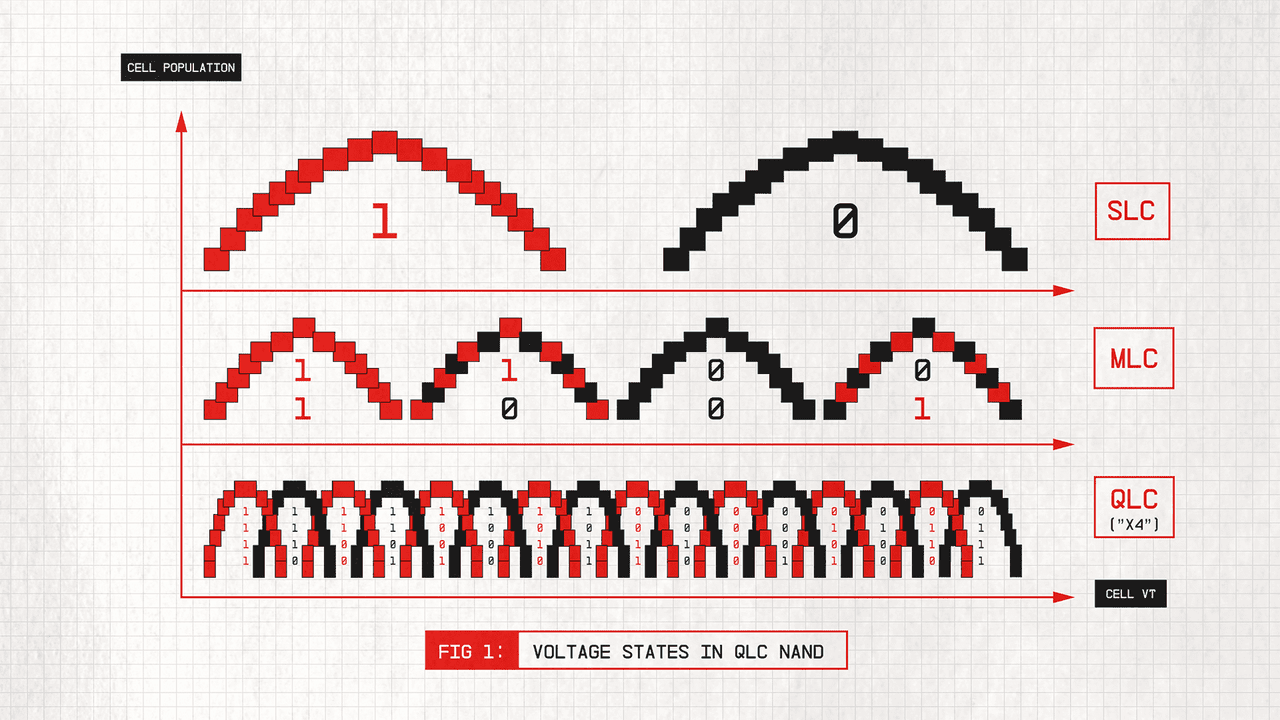
When Sandisk and Toshiba introduced the first commercial product based on Multi-Level Cell (MLC) technology in 2001, it marked a revolutionary shift in Flash memory design.
"By storing two bits of data in each cell, MLC doubled storage capacity and slashed the cost of NAND flash, making it the preferred storage solution for everything fast, small, and portable," Dr. Sharon said.
But the breakthrough begged the question of how far NAND scaling could really go.
Just a year later, M-systems (later acquired by Sandisk) teamed up with Tel Aviv University to explore a NAND Flash solution that could store four bits per cell.
The challenge wasn't just one of physics. Squeezing 16 voltage states into a narrow voltage window could only work by overlapping them, meaning that any margin for distinction would be lost. The level of precision needed to correct errors was considered impossible.

But the theoretical framework defined by information theory suggested this was achievable, and Dr. Sharon's Ph.D. research on Low Density Parity Check (LDPC) error correction codes was a perfect fit to take on the challenge.
By 2006, a fully functional controller was developed, marking the first time LDPC codes and advanced digital signal processing algorithms were applied to Flash. M-Systems announced the company's breakthrough proprietary x4 technology, enabling what became the world's first QLC NAND—a milestone that defined the future of Flash storage.
Back to the future
Twenty years later, Dr. Sharon's pioneering work has not slowed down; on the contrary.
The aggressive shrinking of NAND alongside the introduction of 3D stacking has made Flash a fundamentally "noisier" media and one that is harder to manufacture with process uniformity. At the same, applications demand even more—higher performance, lower power, and better reliability.
"There's a growing gap between NAND's raw capabilities and the needs of end users," Dr. Sharon said.
He explained that in Flash media, individual pages, blocks, and dies within the same device will see variations due to manufacturing processes, which gets harder to control with scaling. There are also operational factors, such as how many times a cell has been programmed, how much time has elapsed since the data was stored, or the write and read temperatures, all factors that influence the memory characteristics and data reliability.

"To keep pushing the boundaries of advanced math and algorithms, we're adopting new tools and methodologies," Dr. Sharon said. "Today, there might be 30 parameters we need to take into account every time a bit is read in order to infer the optimal Flash operational parameters —temperature, the age of the data, the memory wear, the physical address, and so on. It's too many parameters to build a mathematical model for digital signal processing, but it's the perfect use case for machine learning and AI-based inferencing. We're always expanding our toolkit as the challenges grow from generation to generation."
As Flash storage evolves, innovation isn't confined to one field; it thrives at the intersection of many—information and coding theory, Digital Signal Processing (DSP), math and statistics, machine learning, cryptography, and hardware design. By bringing these fields together, Dr. Sharon and his team can develop coding schemes that enable Flash to continue scaling, even as physical limits are tested.
"We have a unique team in the industry, built on decades of joint innovation and expertise," Dr. Sharon said. "We are able to tailor efficient algorithmic solutions according to the specific demands of each product—from ultra high-density storage solutions to high bandwidth and ultra low latency memory solutions for emerging AI workloads."
Building the future
As Sandisk continues to push the boundaries with innovations like UltraQLC and High Bandwidth Flash, it's those once-theoretical coding schemes that have become the backbone of modern memory; their impact unmistakably real.
"What we do touches millions of lives—encoding and decoding trillions of 1s and 0s saved on digital devices every second of every day," Dr. Sharon said. "That's what motivates us; knowing that the algorithms invented and developed by our team are safeguarding the data of people all over the world."
Author
Ronni Shendar
November 25, 2025
[5 min read]